
LINTEC to Open New Research Facility, “Semiconductor Solutions Lab,” in Fukuoka Prefecture, Japan
LINTEC has decided to open a new research facility, the Semiconductor Solutions Lab, on a site adjacent to the Fukuoka
LINTEC has decided to open a new research facility, the Semiconductor Solutions Lab, on a site adjacent to the Fukuoka

LINTEC announces the company will invest approximately 8 billion yen to establish a new research and development hub on Port
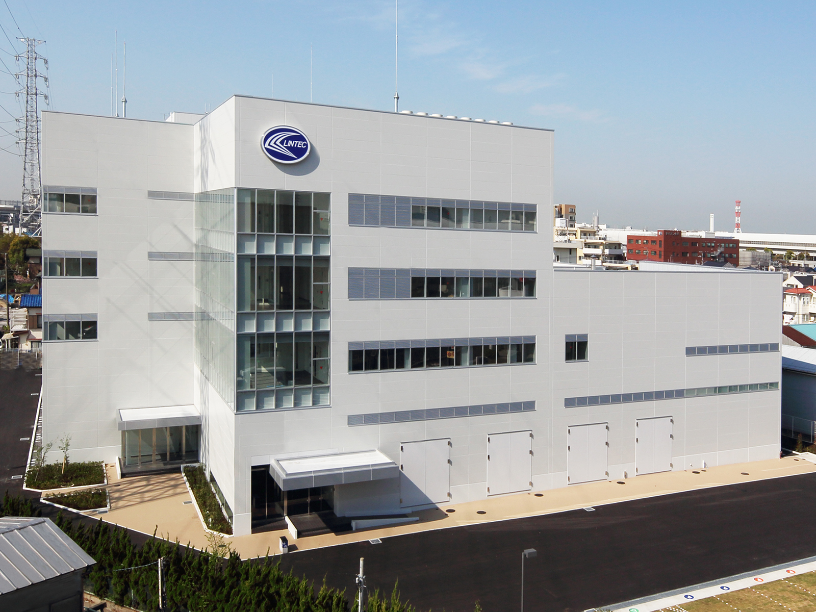
Great news for our customers! LINTEC Corporation has opened a new Advanced Development Center in Japan to accelerate innovation in
The semiconductor industry is evolving rapidly, driven by demand for smaller, faster, and more efficient electronic devices. At the core
The semiconductor industry has moved past simple miniaturization. We are now in the age of heterogeneous integration and chiplets, where
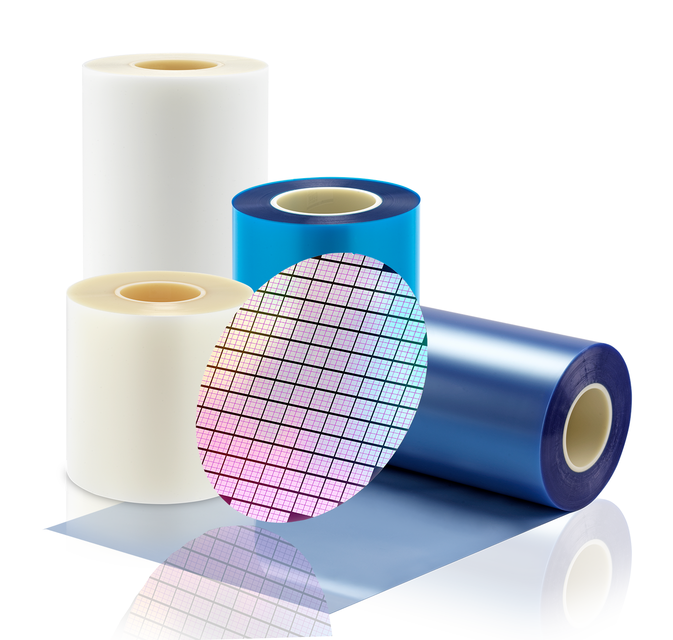
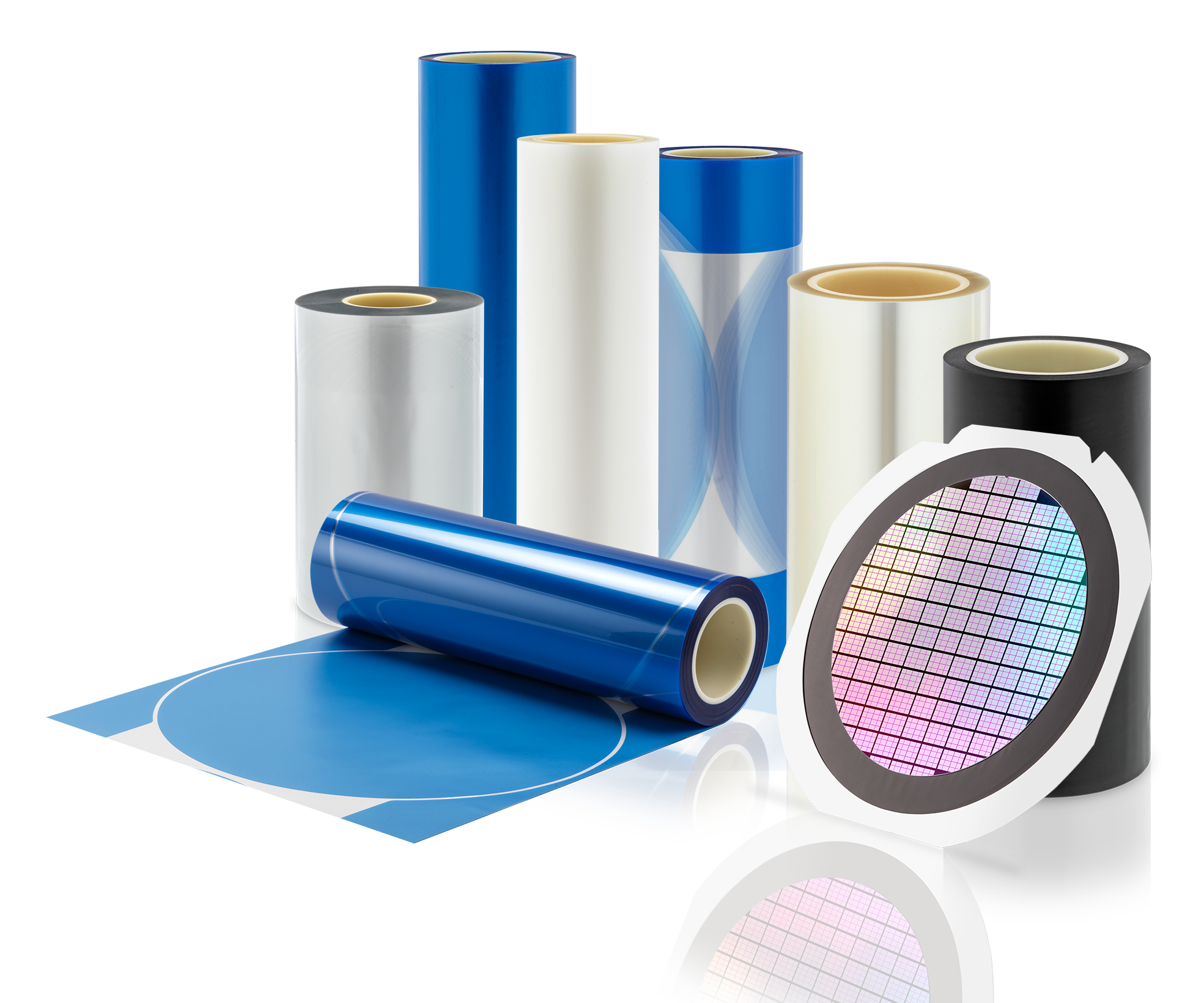
In the fast-evolving semiconductor industry back-grinding tape has become a mission-critical consumable in wafer thinning processes. As chip architectures become

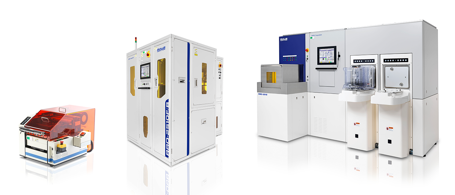
A few days ago, we had a different kind of photoshoot. Instead of models, our semi-automatic machines and tapes were

LINTEC has developed Pattern Coating Before Lamination (PCBL), a process for the back grinding of semiconductor wafers that reduces thickness

It was a great pleasure to have the opportunity to introduce LINTEC’s Tape x Equipment solutions to Minister Aiwanger. Bavaria
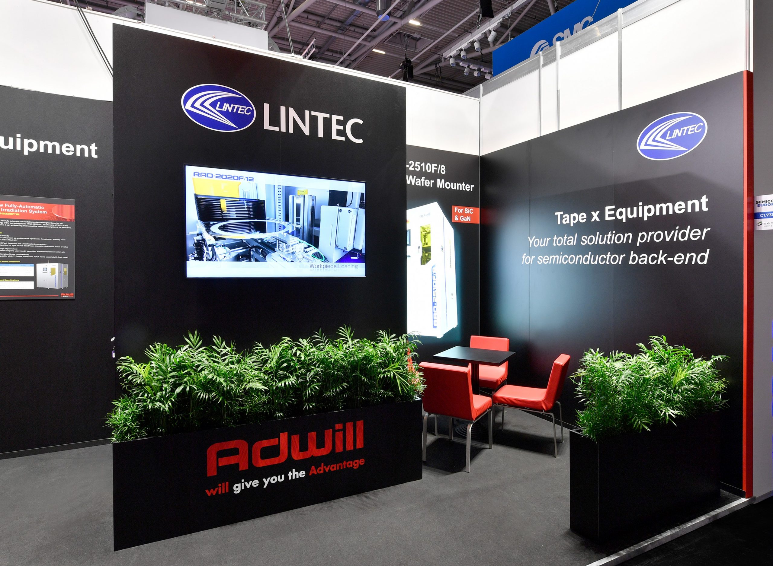
From November 18-21, we’ll be on site and look forward to engaging conversations with partners, customers, and industry peers.