The semiconductor industry has moved past simple miniaturization. We are now in the age of heterogeneous integration and chiplets, where how you cut the wafer is just as important as how you design the circuit. At the heart of this back-end revolution lies a high-tech consumable that often doesn’t get the spotlight it deserves: semiconductor grade dicing tape. While often overlooked, this material has become a critical enabler of modern chip manufacturing performance.
For procurement managers, process engineers, and fab operators in Europe, the choice of dicing tape is no longer just about stickiness. It is about yield, throughput, and the ability to handle wafers thinner than a human hair.
In this context, selecting the right partner is just as important as selecting the right product. LINTEC Advanced Technologies (Europe) GmbH, based in Munich, is redefining what manufacturers can expect from semiconductor dicing tape with its unique “Tape × Equipment” philosophy.
What is Semiconductor Dicing Tape?
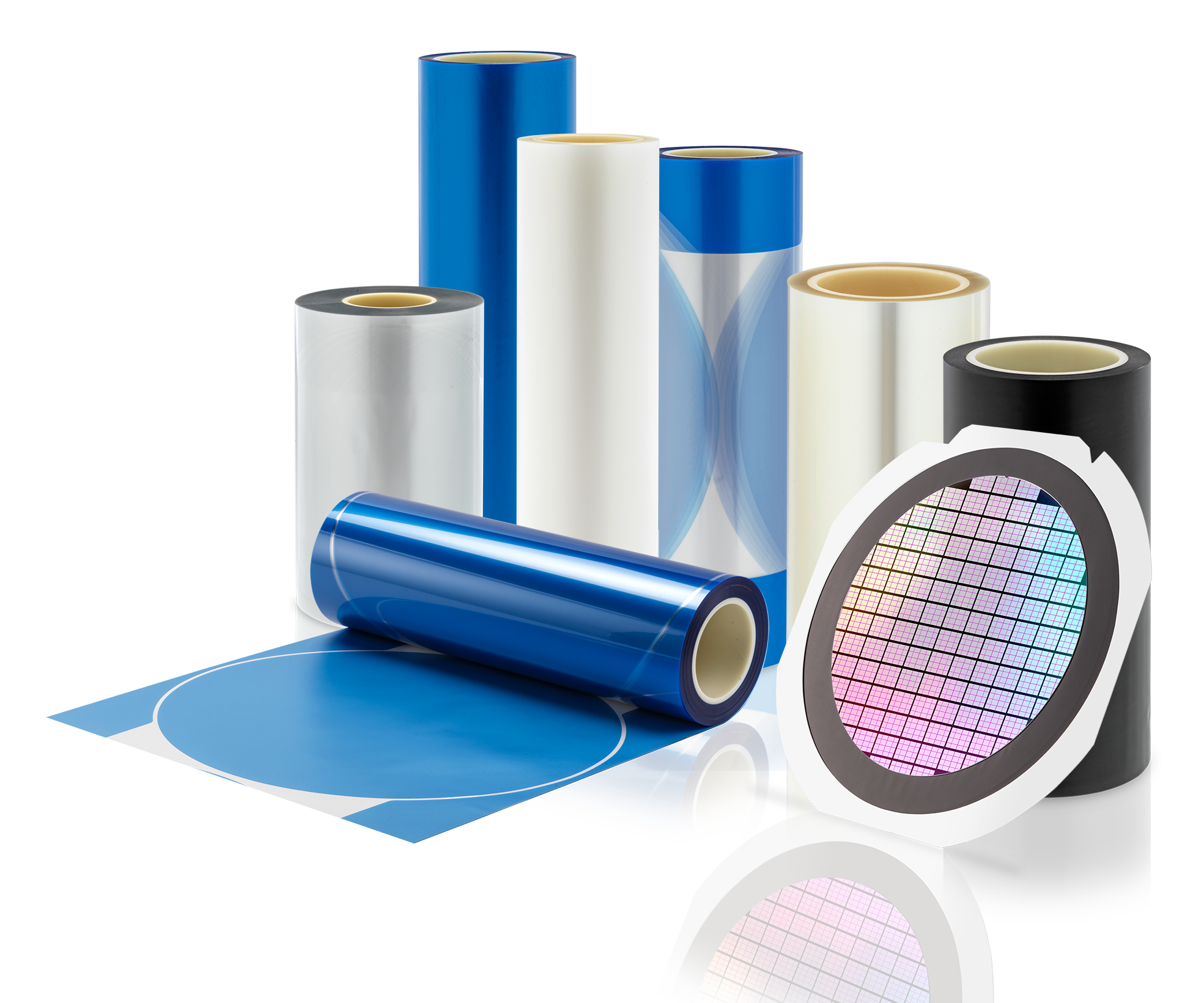
Before diving into the specific advantages of LINTEC’s Munich operations, it is crucial to understand the physics of the process. Semiconductor dicing tape (often also referred to as wafer mounting tape) is a pressure-sensitive adhesive film used to hold a wafer in place during the sawing or “dicing” process. The wafer is cut into thousands of individual dies (chips). Despite its apparent simplicity, the performance of this tape directly influences yield, defect rates, and downstream process stability.
The Three Critical Functions of Dicing Tape:
Hold: It must secure the wafer firmly during contact with a dicing-blade rotating at high speed and water cooling.
Protect: It acts as a shock absorber, preventing micro-cracks on the fragile substrate.
Release: After dicing, the tape must release the individual chips without residue so robots can pick them up for packaging.
The industry is more and more shifting towards UV-curable tapes. Unlike traditional non-UV tapes, UV-curable tapes offer high adhesion during cutting and near-zero adhesion after UV light exposure, making them mandatory for brittle material and (ultra-) thin chips. This shift reflects the increasing fragility and value of modern wafers, where even microscopic damage can lead to significant losses.
The “Tape x Equipment” Synergy
Most suppliers sell tape. Some also sell equipment. LINTEC is special because we not only design both products under one roof, but we also have our very own team of equipment and tape engineers standing by to support you. This integrated approach ensures that materials and machinery are not optimized in isolation, but as a fully synchronized system.
For purchasing managers and engineers visiting this website, specifications matter. LINTEC Munich offers a portfolio that covers the full spectrum of backend manufacturing.
For Advanced Packaging
European fabs are leading in specialized packaging like MEMS and power electronics. These applications demand especially high mechanical stability and contamination control during dicing.
D-5XX Series: Specifically designed for package dicing, these tapes offer high adhesion (e.g. D-510TC: 13,000 mN/25mm) to securely hold rough-molded substrates during dicing, while allowing easy pick-up after UV to prevent residues and chipping.
D-8XX Anti-Static Series: Static discharge can kill chips instantly. LINTEC’s anti-ESD tape series (e.g. D-841) offers a surface resistivity of 3.9×10¹¹ Ω/□, draining static before it builds up.
For Laser Dicing
LINTEC offers a broad variety of tapes and expertise for Stealth Dicing™ from circuit-side, Stealth Dicing™ through tape, and for full-cut laser dicing processes. Each of these processes places unique demands on the optical and mechanical properties of the tape.
Exemplary:
D-765 (for full-cut laser dicing): The tape uses a special elastomer as base material that absorbs the shock of laser ablation, preventing tearing of the tape, as well as re-depositing of debris on the chip surface.
D-455H (for Stealth Dicing™): Transparency is key for Stealth Dicing™, especially for Stealth Dicing™ through dicing tape. LINTEC’s tapes achieve 92% transmittance at 1400 nm, allowing the laser to perfectly focus through the tape without energy loss.
People Also Ask
Q: What is the advantage of UV-curable dicing tape?
A: UV-curable tape (like LINTEC’s D-series) is ideal for high-yield, thin-wafer processing. UV light breaks the polymer chains in the adhesive, reducing adhesion strength by up to 90%. This allows for easy “pick-up” without residues, die-chipping or cracking.
Q: How does LINTEC Munich support equipment integration?
A: Unlike tape-only suppliers, LINTEC offers a “showroom” in Munich where customers can test our dicing tape on live equipment (lamination, peeling, mounting, UV irradiation) before making a purchase decision. This hands-on validation significantly reduces process risk and accelerates implementation in production environments.
Why Your Fab Needs a “Total Solution Provider”
Purchasing semiconductor dicing tape is not a commodity transaction – it is a technical partnership. LINTEC’s value proposition is built on the strength of our integrated Adwill ecosystem, which combines three core competencies:
Consulting: Our equipment and tape engineers work closely with you to solve any process challenge – from root-cause analysis to optimizing your dicing performance.
Automation: We design machines that are almost unlimited in their modifiability and can be precisely tailored to your specific process and production requirements.
Chemistry: Adhesive formulation and application are our core competencies, enabling stable, consistent, and high-precision results.
By combining these disciplines, LINTEC moves beyond the role of a supplier and becomes a long-term technology partner. Because our consumables and capital equipment are engineered to work with each other – not against each other – LINTEC delivers the lowest Total Cost of Ownership (TCO) for every customer.
Conclusion
As the semiconductor industry continues to evolve, the margin for error is shrinking toward zero. Semiconductor dicing tape has shifted from being a passive holding material to becoming an active contributor to overall yield. In an environment defined by complexity and precision, incremental improvements at the material level can have exponential effects on overall productivity.
At LINTEC Advanced Technologies (Europe) GmbH in Munich, we are not simply selling tape – we are delivering reliability at the heart of Europe. Our “Tape x Equipment” model, combined with our highly advanced Adwill products, provides the precision required for the next generation of AI, automotive, and IoT chips.
If you are experiencing issues with tape performance or struggling to find adequate support, it is time to look beyond the spec sheet. It is time to look at the synergy.