In the fast-evolving semiconductor industry back-grinding tape has become a mission-critical consumable in wafer thinning processes. As chip architectures become more compact and advanced, especially with AI, IoT, EV, and chiplet-based systems, the demand for ultra-thin wafers continues to rise.
For procurement managers and process engineers in Europe, the challenge isn’t just finding a back grinding tape; it is finding a solution that is customized to ones individual needs.
LINTEC Advanced Technologies (Europe) GmbH, based in Munich and part of LINTEC Corporation in Japan, is setting the benchmark for the industry. By integrating high-performance tapes with advanced equipment, LINTEC maximizes quality and efficiency across various aspects of semiconductor production. This synergy ensures consistent quality and enhanced productivity, keeping pace with the ever-evolving manufacturing landscape.
Why Standard Back-Grinding Tape Fails in Advanced Packaging
To understand the value of the LINTEC solution, we must first look at the physics of wafer thinning. Traditional back-grinding tape serves a simple purpose: protect the circuitry on the front side of the wafer while the backside is ground down to 50µm or less.
However, the rise of hybrid bonding and bump wafers has introduced a critical flaw in standard processes: Topography Variation.
When you apply standard tape over a wafer with copper pillars (bumps), the tape cannot fill the gaps perfectly. This leads to “step height differences.” When the grinding wheel hits the wafer, these micro-voids cause uneven pressure distribution. The result? Cracked edges, chipping, and a phenomenon known as “kerf shift” where dies move out of alignment. To prevent this from happening, LINTEC either offers specialized back-grinding tapes suitable to cater for even the most challenging topographies, or a revolutionary concept that was just recently published.
The PCBL Breakthrough (2026)
In February 2026, LINTEC announced a game-changing process to solve this: Pattern Coating Before Lamination (PCBL).
Instead of relying solely on the tape’s buffer layer to absorb topography, LINTEC developed the RAD-3400F/12 Resin Coater. This system applies a UV-curable resin specifically to the bump-free outer periphery of the wafer before the back-grinding tape is applied. This creates a perfectly flat surface. The result is a reduction in thickness variation and cracking, allowing European fabs to push yields higher without upgrading their entire grinding fleet.
Why Back-Grinding Tape Matters
Back-grinding tape is a crucial process in semiconductor manufacturing where the backside of a wafer is ground down to reduce thickness after circuit formation.
During this process, wafers, often thinner than 100 µm, become extremely fragile. Without proper protection, they are vulnerable to:
● Cracks and chipping
● Contamination from grinding debris
● Warpage and stress damage
This is where back-grinding tape plays a vital role.
LINTEC’s solutions are designed to:
● Protect wafer surfaces during grinding
● Prevent contamination from fluids and particles
● Maintain structural integrity of ultra-thin wafers
● Enable clean and damage-free peeling after processing
● Ensure lowest possible TTV after grinding
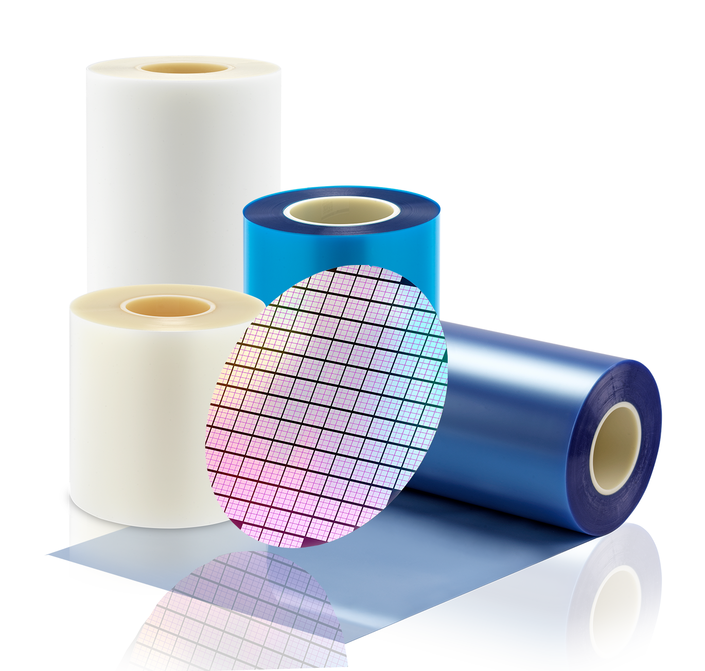
What is Back-Grinding Tape?
Back-grinding tape is a pressure-sensitive adhesive film applied to the active (front) side of a semiconductor wafer before the grinding process.
Its primary functions include:
1. Protection – Shields circuits from mechanical damage
2. Stability – Holds wafer firmly during grinding
3. Clean Removal – Ensures residue-free peeling after processing
At LINTEC Corporation, these tapes are part of the Adwill product line, engineered for precision semiconductor applications.
Key Benefits of LINTEC Back-Grinding Tape
Superior Wafer Protection: Prevents micro-cracks, scratches, and contamination during grinding.
Stress Control & Warpage Reduction: Advanced adhesive formulations distribute stress evenly, reducing wafer bow.
High Precision Thickness Control: Uniform tape thickness and a very low TTV ensures consistent grinding results.
Clean Peeling Process: UV-curable tapes allow residue-free removal, reducing post-processing steps.
Improved Yield: Minimizes defects and increases usable die output.
Applications Across Industries
Back-grinding tape is essential across multiple semiconductor sectors:
1. Consumer Electronics
● Smartphones
● Tablets
● Wearables
2. Automotive (EV & ADAS)
● Power modules
● Sensors
● Control units
3. Industrial IoT
● Smart factories
● Robotics
4. AI & High-Performance Computing
● GPUs
● AI accelerators
● Data center chips
Back-Grinding Tape – Types & Technologies
1. UV-Curable Back-Grinding Tape (E-Series)
E-Series is a flagship solution of UV-curable grinding-tapes for advanced semiconductor manufacturing. LINTEC holds a strong global position among the top three suppliers of UV-curable back-grinding tape worldwide and maintains a leading role with numerous patents, including advanced DBG and SDBG solutions.
Key Features:
● High adhesion during grinding
● Adhesion reduction after UV exposure
● Easy peel-off with minimal stress
● Ideal for ultra-thin wafers
UV irradiation significantly reduces adhesion, enabling safe removal without damaging delicate wafers.
Use Cases:
● Advanced logic chips
● Memory devices
● Thin wafers (<100 µm)
● Bump wafers
2. Non-UV Back-Grinding Tape (P-Series)
The P-Series is designed for applications where UV processing is not required.
Key Features:
● Stable adhesion without UV exposure
● Cost-effective for standard processes
● Suitable for thicker wafers
Use Cases:
● Legacy semiconductor processes
● Less sensitive wafer structures
LINTEC Munich’s “Tape x Equipment” Advantage
LINTEC Corporation and LINTEC Advanced Technologies (Europe) GmbH has a major advantage that is rare in the industry: their physical presence in the heart of Europe, Munich (Konrad-Zuse-Platz 1) and their integrated solution model.
In the semiconductor supply chain, a tape is only as good as the lamination. If you apply a premium back-grinding tape with a machine that has poor tension control, you will get air gaps (bubbles) and breakage.
To ensure quality, LINTEC Advanced Technologies (Europe) GmbH offers a fully integrated system:
Components:
● Back-grinding, dicing and special tapes
● Laminators
● Peelers
● Wafer mounters
● UV irradiation systems
This integration ensures:
● Perfect compatibility between tape and equipment
● Reduced process variability
● Higher yield and throughput
LINTEC emphasizes that combining tape chemistry with machine engineering creates optimized production workflows. For a German or European fab manager, this means short response times. Field Support Engineers can be on-site the next day for troubleshooting, maintenance, or repairs, while tape specialists assist with trials, analysis, and process optimization directly in your fab.
Why Choose LINTEC Munich?
LINTEC Advanced Technologies (Europe) GmbH stands out for several reasons:
1. Total Solution Provider: Offers both consumables and equipment under one ecosystem.
2. European Presence: Our Munich-based operations ensure fast support.
3. Customization: Solutions tailored to specific fab requirements.
4. Proven Industry Expertise: Installed in all major semiconductor fabs across Europe.
How to Choose the Right Back-Grinding Tape
For procurement managers and engineers, selecting the right tape involves:
1. Wafer Thickness
● Thin wafers, SiC wafers, wafers with sensitive surfaces, bump wafers, DBG or SDBG processes → UV-curable (E-Series)
● Thick or less delicate wafers → Non-UV (P-Series)
2. Process Compatibility
Ensured compatibility with:
● Laminators
● UV systems
● Peeling equipment
3. Adhesion Strength
Balance between:
● Strong hold during grinding
● Easy release after process
4. Contamination Control
Choose tapes that eliminate residue and debris.
Frequently asked questions
What is back-grinding tape used for?
Back-grinding tape protects semiconductor wafers during thinning by preventing damage, contamination, and stress.
Why is UV-curable tape important?
It allows strong adhesion during grinding and easy removal after UV exposure, reducing wafer damage.
What is the difference between E-Series and P-Series?
● E-Series: UV-curable, ideal for thin wafers, SiC wafers, wafers with sensitive surfaces, bump wafers, DBG or SDBG processes
● P-Series: Non-UV, suitable for thick or less delicate wafers
Does back-grinding tape affect yield?
Yes. High-quality tape significantly improves yield by reducing defects and wafer breakage.
Can back-grinding tape eliminate cleaning steps?
Yes, advanced tapes can prevent contamination, reducing or eliminating post-grinding cleaning.
What is the difference between back-grinding tape and dicing tape?
Back-grinding tape is designed with special adhesive-layers and basefilms to absorb grinding wheel pressure and protect the wafer surface topography during mechanical thinning. Dicing tape is thinner, has a higher tack (stickiness) to hold the wafer during sawing, and is designed to expand for die separation. LINTEC offers distinct product lines for both processes.
How do you remove back-grinding tape without breaking the wafer?
LINTEC utilizes UV irradiation systems. After grinding, the tape is exposed to UV light, which breaks the cross-links in the adhesive polymer chain. This reduces the adhesive strength (peel force) drastically, allowing the back-grinding tape to be removed by peeling / delamination systems like LINTEC’s RAD-3000 series without exerting mechanical stress on the thin die.
Where can I buy LINTEC back-grinding tape in Europe?
Directly through LINTEC Advanced Technologies (Europe) GmbH in Munich, Germany. We handle distribution, technical consulting, and after-sales service for the entire EMEA region. Our showroom in Munich is also available for process validation trials.
Securing Your Supply Chain
With increasing wafer thinness, complex chip architectures, and higher production demands, manufacturers must invest in high-performance materials and integrated solutions.
LINTEC Advanced Technologies (Europe) GmbH delivers exactly that through its advanced E-Series and P-Series back-grinding tapes combined with precision equipment.
For industry professionals, engineers, and procurement managers, choosing LINTEC means:
● Higher yield
● Lower defect rates
● Future-ready semiconductor processes
The era of simple protective film is over. Today, back-grinding tape is an active contributor to die strength and singulation quality.
LINTEC Munich offers three distinct advantages that mitigate risk for the buyer:
1. Technology: The new PCBL process (RAD-3400F/12) solves the bump topography issue that standard tapes cannot.
2. Engineering: High-modulus substrates prevent kerf shift in DBG processes.
3. Proximity: A local European headquarters with a showroom that is ready for customer-trials, a large amount of sample-tapes in stock, local tape- and equipment specialists, and rapid response times.
If you are facing troubles in finding a trustworthy partner for your semiconductor back-end and assembly processes, it is time to move beyond consumables procurement and look at a total solution partner. LINTEC has the tape, the equipment, and the local expertise to keep your fab running at peak efficiency.